After the etching process, holes are drilled into the turnkey pcb assembly to accommodate components and connectors. These holes are plated with a thin layer of copper to ensure strong electrical connections. The precision required in this step is critical to guarantee that components fit perfectly and that signals pass through without interference.
Solder Mask and Silkscreen – Adding the Final Touches:
To protect the copper traces and help with component placement, a solder mask is applied over the PCB. This green or sometimes red layer shields the conductive pathways from environmental factors and prevents unwanted short circuits. The silkscreen layer is also added, providing labels and markings to guide assembly and maintenance.
Quality Control – A Crucial Step:
Quality control is an integral part of PCB fabrication. Inspection processes include automated optical inspection (AOI) and manual checks to ensure that there are no defects, misalignments, or missing components. These rigorous quality checks help guarantee the reliability of the final product.
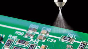
Testing and Assembly – Bringing the PCB to Life:
Once the PCB is fabricated and deemed flawless, it undergoes rigorous testing to confirm that all electrical connections are functioning as intended. The PCB is then ready for assembly, where electronic components are soldered onto their designated positions. This step transforms the inert board into a fully functional electronic circuit.